How Are Computer Chips Made? From Sand to Silicon…
Journey to the Centre of the Earth
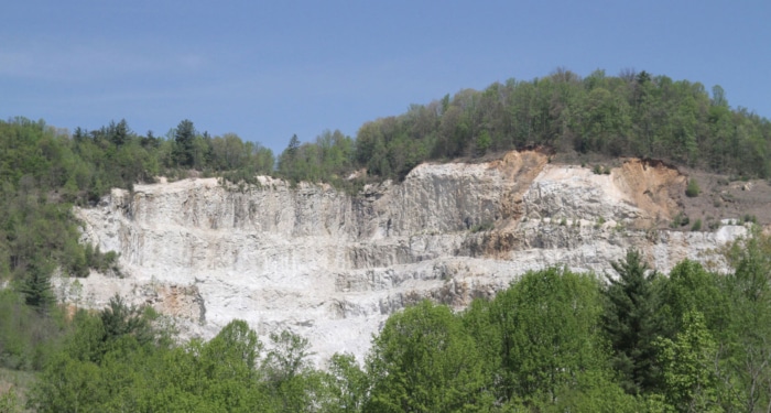
Long before it started to work its magic in your console, your computer chip began life deep in the ground, eventually rising to the surface in the form of milky white sand. It’s the kind of sand you might see while basking on a hot beach in Anguilla, although this is usually mined from quarries in slightly less glamorous locations. It’s rich in quartz, which is also known as silicon or silica. This is the raw material that forms the basis of a semiconductor. But to manufacture the most advanced chips needed in computers, there’s one place on earth that you need to visit.
If you head to western North Carolina, in the foothills of the Appalachian Mountains, there’s a town so rich in minerals that they built a mineral museum. Driving into the town, a big sign tells you you’re in Mineral City. Spruce Pine has little over 2,000 residents, and sand is its main export (it’s also known as white gold). This unique geographical location is ideal for producing the silica needed in the production of computer chips. Due to its glimmering quality, it’s also used in the Augusta National Golf Club, giving the bunkers their brilliant whiteness.
Pure silicon is needed for advanced semiconductors for computers, consoles, graphics cards and fibre optic cables. The chips in your toaster can deal with a grittier type of silicon.
Shockley’s Discovery
It wasn’t until the mid-1950s that an engineer called William Shockley – who was part of the team that invented the transistor – discovered that silicon could be used in the production of semiconductors. Before that, it was used to make glass. In fact, the largest telescope in the world was made using Spruce Pine sand. The mirror, built in the 1930s, weighs 20 tonnes and is still in use today.
Made Under a Golden Light
Making semiconductors is a meticulous process that needs nothing less than absolute precision. The silica for computer chips needs to be 99.9999999999% pure, which knocks the socks off the meagre 99.999999 silicon percentage purity for solar panels. To get to this level, it’s treated with chemicals, such as silicon tetrachloride, then trichlorosilane – which is further treated to become polysilicon. It’s this polysilicon that becomes the chip. But first, it needs to be cooked.

To retain its purity, the silicon has to be melted in a furnace in a semiconductor fabrication plant (fab) containing a crucible. It’s the crucible rather than the chip that’s made from the sand found in Spruce Pine. A company called Unimin has a monopoly on this white sand, and it’s not cheap, at around US$10,000 (approx. £7,500) per tonne. The crucibles look fairly unremarkable when produced, not too dissimilar to an Ikea soup bowl.
To make the wafers on which the chips are made, technicians use a process called the Czochralski method. A seed crystal is dipped into the molten silicon with a rod and slowly pulled out at controlled temperatures, revealing a pure silicon ingot known as a boule. The boule is then sliced into thin wafers like pepperoni. To control the level of conductivity in the silicon, impurities are added, such as phosphorous or boron. This process is known as doping.
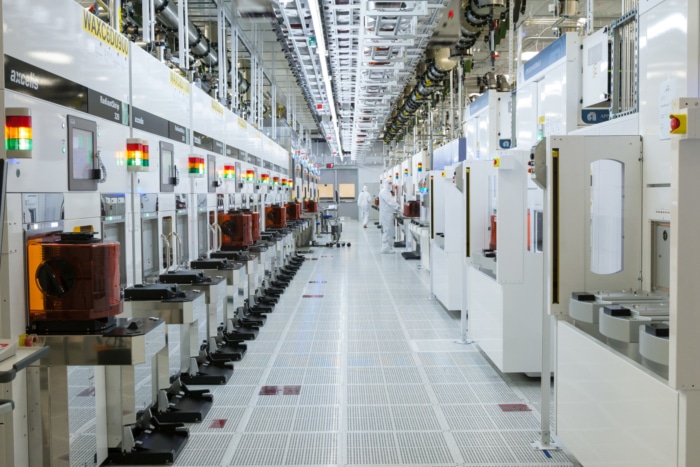
Care is taken to ensure no unwanted impurities come into contact with the wafer. The minutest particle of dust or hair can wreak havoc on the chips and cost the company millions, so wafers are rarely handled by humans, and they swivel around in airtight compartments on monorails in a cleanroom, where the air is filtered and purified. The cleanrooms are thousands of times more sanitary than most manufacturing plants. Technicians wear hazmat-style white suits just like in ET The Extraterrestrial and are air-washed before entering the cleanroom. Unsurprisingly, cleanrooms aren’t cheap to build, and a new fab can cost anywhere from US$1bn to US$3bn.

To create one semiconductor, there are hundreds of steps made over a period of at least three months. Each wafer is refined and polished to give them a mirror-like sheen, which gets rid of any contaminants and makes them both stronger and more flexible. The wafers are covered with levels of insulating and conducting material, then finally topped with a thin photoresist layer. All this is conducted under amber-coloured LEDs. This golden light prevents regular white light from overexposing the photoresist layer.
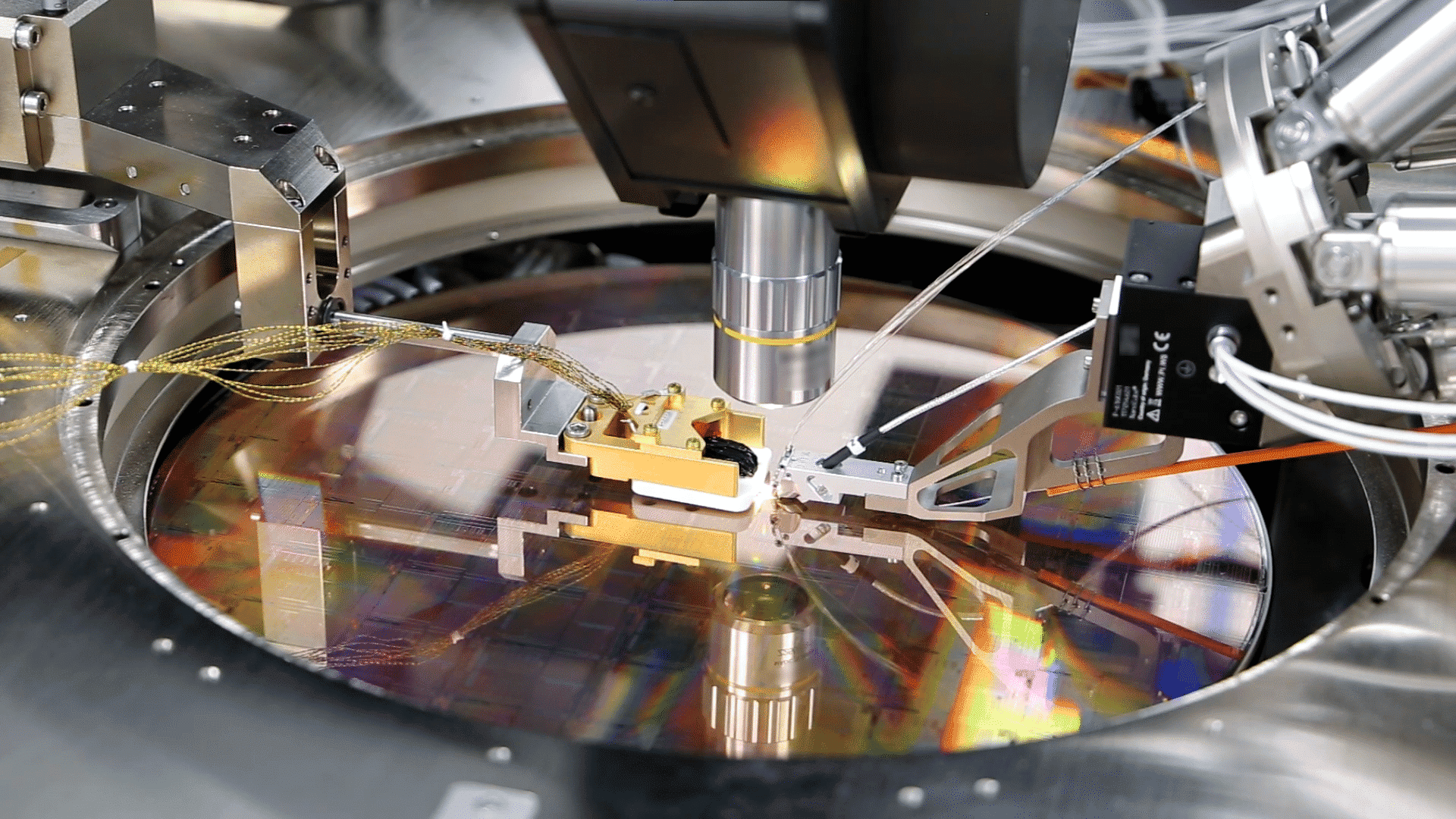
Using UV lithography, a pattern of billions of transistors is transferred from a plate called a photomask to the wafer using light. Then copper is added to connect the transistors into integrated circuits, which are finally sliced into tiny chips. Then they are shipped off to the next leg of their journey to be tested, then transported again to tech-making facilities where they are inserted into the computers in your homes and pockets.
Chip sizes are decreasing rapidly. In May this year, IBM unveiled a complete system-on-a-chip (SoC) smaller than a grain of salt, and in June, Columbia University announced the creation of an injectible single-chip system the size of a dust-mite. It’s only a single-chip system for use in monitoring health, but it’s a huge advancement.
And Back to Sand Again
However, another – perhaps unnerving – development is a design created by researchers at Northwestern University. Reminiscent of an episode of Black Mirror, the researchers have designed a winged microchip with helicopter-style rotors that will be used to monitor various situations such as airborne diseases and human surveillance. The ‘Microflier’ is the size of an ant’s head. Indeed, it is the size of a grain of sand.
Bioelectronics pioneer John Rogers, who helped create the flying chip, said: “We think we’ve beaten biology.”

